 | ÐлекÑÑоннÑй компоненÑ: AN8035 | СкаÑаÑÑ:  PDF PDF  ZIP ZIP |
Äîêóìåíòàöèÿ è îïèñàíèÿ www.docs.chipfind.ru
Voltage Regulators
1
Publication date: December 2001
SFF00007CEB
AN80xx/AN80xxM Series
3-pin, positive output, low dropout voltage regulator (50 mA type)
I Overview
The AN80xx series and the AN80xxM series are 3-
pin, low dropout, fixed positive output type monolithic
voltage regulators. Since their power consumption can
be minimized, they are suitable for battery-used power
supply and reference voltage. 13 types of output voltage
are available; 2V, 2.5V, 3V, 3.5V (SSIP003-P-0000 only),
4V, 4.5V, 5V, 6V, 7V, 8V, 8.5V, 9V, and 10V.
I Features
· Input/output voltage difference: 0.3V max.
· Output current of up to 50mA
· Low bias current: 0.6mA typ.
· Output voltage: 2V, 2.5V, 3V, 3.5V (SSIP003-P-0000
only), 4V, 4.5V, 5V, 6V, 7V, 8V, 8.5V, 9V, and 10V
· Built-in overcurrent protection circuit
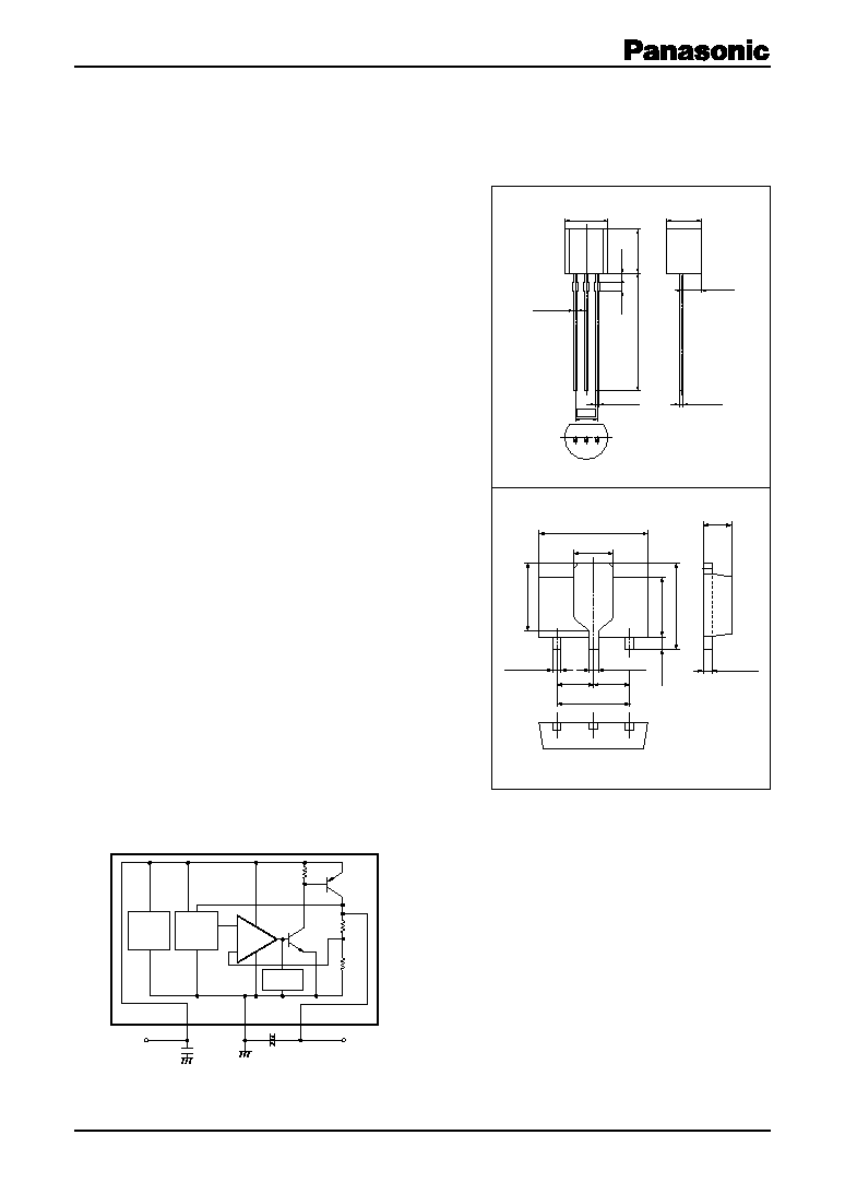
SSIP003-P-0000
AN80xx series
Unit: mm
AN80xxM series
Unit: mm
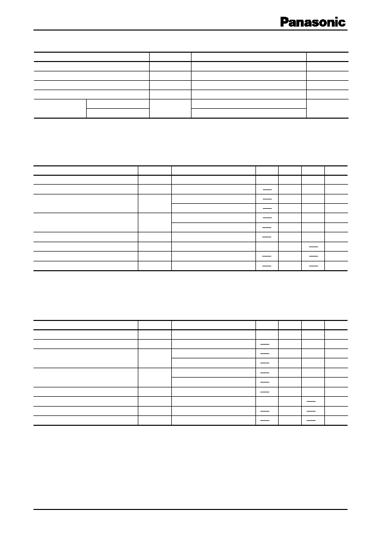
Voltage
Reference
Current
Limiter
Starter
V
O
R
1
R
2
C
OUT
C
IN
R
1
= 5k
C
IN
= 0.33µF
C
OUT
= 10µF
V
I
Note) The number in ( ) shows the pin number for the AN80xx series.
+
Error
Amp.
-
- +
3
(1)
2
(3)
1
(2)
I Block Diagram (AN80xxM series)
HSIP003-P-0000B
5.0±0.2
5.1±0.2
13.5±0.5
(1.0)
(1.0)
4.0±0.2
2.3±0.2
0.6±0.15
0.43
+0.1
0.05
2.54
0.43
+0.1
0.05
2
1
3
2.6 typ.
1.6 max.
1.8 max.
4.6 max.
3.0
1.5
1.5
3
2
1
0.48 max.
0.58 max.
0.44 max.
4.25 max.
2.6 max.
0.8 min.
1: Input
2: Output
3: GND
1: Output
2: GND
3: Input
Note) The packages (SSIP003-P-0000 and HSIP003-
P-0000B) of this product will be changed to
lead-free type (SSIP003-P-0000S and
HSIP003-P-0000Q). See the new package di-
mensions section later of this datasheet.
AN80xx/AN80xxM Series
2
SFF00007CEB
I Absolute Maximum Ratings at T
a
= 25°C
I Electrical Characteristics at T
a
= 25°C
· AN8002, AN8002M (2V type)
V
I
I
CC
P
D
T
opr
T
stg
Supply voltage
Supply current
Power dissipation
Operating ambient temperature
Storage temperature
Parameter
Symbol
Rating
20
100
650 *
-30 to +80
-55 to +150
-55 to +125
* AN80xxM series is mounted on standard board (glass epoxy: 20mm
× 20mm × t1.7mm with Cu foil of 1cm
2
or more).
AN80xx series
AN80xxM series
V
mA
mW
°C
°C
Unit
Parameter
Symbol
Conditions
Min
Typ
Max
Output voltage
V
O
2.08
V
2
T
j
= 25°C
Line regulation
REG
IN
mV
V
I
= 2.5 to 8V, T
j
= 25°C
Load regulation
REG
L
20
mV
I
O
= 1 to 40mA, T
j
= 25°C
mV
Minimum input/output voltage difference
V
DIF(min)
V
0.06
V
I
= 1.9V, I
O
= 20mA, T
j
= 25°C
V
V
I
= 1.9V, I
O
= 50mA, T
j
= 25°C
I
O
= 1 to 50mA, T
j
= 25°C
mA
0.6
I
O
= 0mA, T
j
= 25°C
Note 1) The specified condition T
j
= 25°C means that the test should be carried out within so short a test time (within 10ms) that the
characteristic value drift due to the chip junction temperature rise can be ignored.
Note 2) Unless otherwise specified, V
I
= 3V, I
O
= 20mA and C
O
= 10µF.
Bias current
I
Bias
dB
V
I
= 3 to 5V, f = 120Hz
Ripple rejection ratio
RR
µV
Output noise voltage
V
no
mV/
°C
0.1
f
= 10Hz to 100kHz
Output voltage temperature coefficient
V
O
/T
a
T
j
= -30 to +125°C
25
40
0.2
0.3
1
1.92
62
0.12
2
7
10
60
74
Unit
· AN8025, AN8025M (2.5V type)
V
O
V
REG
IN
mV
REG
L
mV
mV
V
DIF(min)
V
V
mA
I
Bias
dB
RR
µV
V
no
mV/
°C
V
O
/T
a
2.6
2.5
T
j
= 25°C
V
I
= 3 to 8.5V, T
j
= 25°C
20
I
O
= 1 to 40mA, T
j
= 25°C
0.07
V
I
= 2.4V, I
O
= 20mA, T
j
= 25°C
V
I
= 2.4V, I
O
= 50mA, T
j
= 25°C
I
O
= 1 to 50mA, T
j
= 25°C
0.6
I
O
= 0mA, T
j
= 25°C
V
I
= 3.5 to 5.5V, f = 120Hz
0.13
f
= 10Hz to 100kHz
T
j
= -30 to +125°C
25
50
0.2
0.3
1
2.4
60
0.12
2.5
8
12.5
65
72
Parameter
Symbol
Conditions
Min
Typ
Max
Output voltage
Line regulation
Load regulation
Minimum input/output voltage difference
Note 1) The specified condition T
j
= 25°C means that the test should be carried out within so short a test time (within 10ms) that the
characteristic value drift due to the chip junction temperature rise can be ignored.
Note 2) Unless otherwise specified, V
I
= 3.5V, I
O
= 20mA and C
O
= 10µF.
Bias current
Ripple rejection ratio
Output noise voltage
Output voltage temperature coefficient
Unit
AN80xx/AN80xxM Series
3
SFF00007CEB
I Electrical Characteristics at T
a
= 25°C (continued)
· AN8003, AN8003M (3V type)
· AN8035(3.5V type)
V
O
V
REG
IN
mV
REG
L
mV
mV
V
DIF(min)
V
V
mA
I
Bias
dB
RR
µV
V
no
mV/
°C
V
O
/T
a
3.12
3
T
j
= 25°C
V
I
= 3.5 to 9V, T
j
= 25°C
25
I
O
= 1 to 40mA, T
j
= 25°C
0.07
V
I
= 2.9V, I
O
= 20mA, T
j
= 25°C
V
I
= 2.9V, I
O
= 50mA, T
j
= 25°C
I
O
= 1 to 50mA, T
j
= 25°C
0.6
I
O
= 0mA, T
j
= 25°C
V
I
= 4 to 6V, f = 120Hz
0.15
f
= 10Hz to 100kHz
T
j
= -30 to +125°C
30
50
0.2
0.3
1
2.88
58
0.12
3
9
15
70
70
Parameter
Symbol
Conditions
Min
Typ
Max
Output voltage
Line regulation
Load regulation
Minimum input/output voltage difference
Note 1) The specified condition T
j
= 25°C means that the test should be carried out within so short a test time (within 10ms) that the
characteristic value drift due to the chip junction temperature rise can be ignored.
Note 2) Unless otherwise specified, V
I
= 4V, I
O
= 20mA and C
O
= 10µF.
Bias current
Ripple rejection ratio
Output noise voltage
Output voltage temperature coefficient
Unit
V
O
V
REG
IN
mV
REG
L
mV
mV
V
DIF(min)
V
V
mA
I
Bias
dB
RR
µV
V
no
mV/
°C
V
O
/T
a
yp
1
3.64
3.5
T
j
= 25°C
V
I
= 4 to 9.5V, T
j
= 25°C
30
I
O
= 1 to 40mA, T
j
= 25°C
0.07
V
I
= 3.4V, I
O
= 20mA, T
j
= 25°C
V
I
= 3.4V, I
O
= 50mA, T
j
= 25°C
I
O
= 1 to 50mA, T
j
= 25°C
0.6
I
O
= 0mA, T
j
= 25°C
V
I
= 4.5 to 6.5V, f = 120Hz
0.2
f
= 10Hz to 100kHz
T
j
= -30 to +125°C
40
50
0.2
0.3
1
3.36
57
0.12
3.5
10
20
75
69
Parameter
Symbol
Conditions
Min
Typ
Max
Output voltage
Line regulation
Load regulation
Minimum input/output voltage difference
Note 1) The specified condition T
j
= 25°C means that the test should be carried out within so short a test time (within 10ms) that the
characteristic value drift due to the chip junction temperature rise can be ignored.
Note 2) Unless otherwise specified, V
I
= 4.5V, I
O
= 20mA and C
O
= 10µF.
Bias current
Ripple rejection ratio
Output noise voltage
Output voltage temperature coefficient
Unit
· AN8004, AN8004M (4V type)
V
O
V
REG
IN
mV
REG
L
mV
mV
V
DIF(min)
V
V
mA
I
Bias
dB
RR
µV
V
no
mV/
°C
V
O
/T
a
4.16
4
T
j
= 25°C
V
I
= 4.5 to 10V, T
j
= 25°C
30
I
O
= 1 to 40mA, T
j
= 25°C
0.07
V
I
= 3.8V, I
O
= 20mA, T
j
= 25°C
V
I
= 3.8V, I
O
= 50mA, T
j
= 25°C
I
O
= 1 to 50mA, T
j
= 25°C
0.6
I
O
= 0mA, T
j
= 25°C
V
I
= 5 to 7V, f = 120Hz
0.2
f
= 10Hz to 100kHz
T
j
= -30 to +125°C
40
50
0.2
0.3
1
3.84
56
0.12
3.5
10
20
80
67
Parameter
Symbol
Conditions
Min
Typ
Max
Output voltage
Line regulation
Load regulation
Minimum input/output voltage difference
Note 1) The specified condition T
j
= 25°C means that the test should be carried out within so short a test time (within 10ms) that the
characteristic value drift due to the chip junction temperature rise can be ignored.
Note 2) Unless otherwise specified, V
I
= 5V, I
O
= 20mA and C
O
= 10µF.
Bias current
Ripple rejection ratio
Output noise voltage
Output voltage temperature coefficient
Unit
AN80xx/AN80xxM Series
4
SFF00007CEB
I Electrical Characteristics at T
a
= 25°C (continued)
· AN8045, AN8045M (4.5V type)
· AN8005, AN8005M (5V type)
· AN8006, AN8006M (6V type)
V
O
V
REG
IN
mV
REG
L
mV
mV
V
DIF(min)
V
V
mA
I
Bias
dB
RR
µV
V
no
mV/
°C
V
O
/T
a
4.68
4.5
T
j
= 25°C
V
I
= 5 to 10.5V, T
j
= 25°C
35
I
O
= 1 to 40mA, T
j
= 25°C
0.07
V
I
= 4.3V, I
O
= 20mA, T
j
= 25°C
V
I
= 4.3V, I
O
= 50mA, T
j
= 25°C
I
O
= 1 to 50mA, T
j
= 25°C
0.7
I
O
= 0mA, T
j
= 25°C
V
I
= 5.5 to 7.5V, f = 120Hz
0.23
f
= 10Hz to 100kHz
T
j
= -30 to +125°C
45
50
0.2
0.3
1
4.32
54
0.12
4
11
23
85
66
Parameter
Symbol
Conditions
Min
Typ
Max
Output voltage
Line regulation
Load regulation
Minimum input/output voltage difference
Note 1) The specified condition T
j
= 25°C means that the test should be carried out within so short a test time (within 10ms) that the
characteristic value drift due to the chip junction temperature rise can be ignored.
Note 2) Unless otherwise specified, V
I
= 5.5V, I
O
= 20mA and C
O
= 10µF.
Bias current
Ripple rejection ratio
Output noise voltage
Output voltage temperature coefficient
Unit
V
O
V
REG
IN
mV
REG
L
mV
mV
V
DIF(min)
V
V
mA
I
Bias
dB
RR
µV
V
no
mV/
°C
V
O
/T
a
5.2
5
T
j
= 25°C
V
I
= 5.5 to 11V, T
j
= 25°C
40
I
O
= 1 to 40mA, T
j
= 25°C
0.07
V
I
= 4.8V, I
O
= 20mA, T
j
= 25°C
V
I
= 4.8V, I
O
= 50mA, T
j
= 25°C
I
O
= 1 to 50mA, T
j
= 25°C
0.7
I
O
= 0mA, T
j
= 25°C
V
I
= 6 to 8V, f = 120Hz
0.25
f
= 10Hz to 100kHz
T
j
= -30 to +125°C
50
50
0.2
0.3
1
4.8
52
0.12
4.5
12
25
95
64
Parameter
Symbol
Conditions
Min
Typ
Max
Output voltage
Line regulation
Load regulation
Minimum input/output voltage difference
Note 1) The specified condition T
j
= 25°C means that the test should be carried out within so short a test time (within 10ms) that the
characteristic value drift due to the chip junction temperature rise can be ignored.
Note 2) Unless otherwise specified, V
I
= 6V, I
O
= 20mA and C
O
= 10µF.
Bias current
Ripple rejection ratio
Output noise voltage
Output voltage temperature coefficient
Unit
V
O
V
REG
IN
mV
REG
L
mV
mV
V
DIF(min)
V
V
mA
I
Bias
dB
RR
µV
V
no
mV/
°C
V
O
/T
a
6.24
6
T
j
= 25°C
V
I
= 6.5 to 12V, T
j
= 25°C
45
I
O
= 1 to 40mA, T
j
= 25°C
0.07
V
I
= 5.8V, I
O
= 20mA, T
j
= 25°C
V
I
= 5.8V, I
O
= 50mA, T
j
= 25°C
I
O
= 1 to 50mA, T
j
= 25°C
0.7
I
O
= 0mA, T
j
= 25°C
V
I
= 7 to 9V, f = 120Hz
0.3
f
= 10Hz to 100kHz
T
j
= -30 to +125°C
55
60
0.2
0.3
1.2
5.76
51
0.13
5.5
13
28
105
63
Parameter
Symbol
Conditions
Min
Typ
Max
Output voltage
Line regulation
Load regulation
Minimum input/output voltage difference
Note 1) The specified condition T
j
= 25°C means that the test should be carried out within so short a test time (within 10ms) that the
characteristic value drift due to the chip junction temperature rise can be ignored.
Note 2) Unless otherwise specified, V
I
= 7V, I
O
= 20mA and C
O
= 10µF.
Bias current
Ripple rejection ratio
Output noise voltage
Output voltage temperature coefficient
Unit
AN80xx/AN80xxM Series
5
SFF00007CEB
I Electrical Characteristics at T
a
= 25°C (continued)
· AN8007, AN8007M (7V type)
· AN8008, AN8008M (8V type)
· AN8085, AN8085M (8.5V type)
V
O
V
REG
IN
mV
REG
L
mV
mV
V
DIF(min)
V
V
mA
I
Bias
dB
RR
µV
V
no
mV/
°C
V
O
/T
a
7.28
7
T
j
= 25°C
V
I
= 7.5 to 13V, T
j
= 25°C
50
I
O
= 1 to 40mA, T
j
= 25°C
0.07
V
I
= 6.8V, I
O
= 20mA, T
j
= 25°C
V
I
= 6.8V, I
O
= 50mA, T
j
= 25°C
I
O
= 1 to 50mA, T
j
= 25°C
0.7
I
O
= 0mA, T
j
= 25°C
V
I
= 8 to 10V, f = 120Hz
0.35
f
= 10Hz to 100kHz
T
j
= -30 to +125°C
60
70
0.2
0.3
1.3
6.72
50
0.13
6.5
14
31
120
62
Parameter
Symbol
Conditions
Min
Typ
Max
Output voltage
Line regulation
Load regulation
Minimum input/output voltage difference
Note 1) The specified condition T
j
= 25°C means that the test should be carried out within so short a test time (within 10ms) that the
characteristic value drift due to the chip junction temperature rise can be ignored.
Note 2) Unless otherwise specified, V
I
= 8V, I
O
= 20mA and C
O
= 10µF.
Bias current
Ripple rejection ratio
Output noise voltage
Output voltage temperature coefficient
Unit
V
O
V
REG
IN
mV
REG
L
mV
mV
V
DIF(min)
V
V
mA
I
Bias
dB
RR
µV
V
no
mV/
°C
V
O
/T
a
yp
8.32
8
T
j
= 25°C
V
I
= 8.5 to 14V, T
j
= 25°C
55
I
O
= 1 to 40mA, T
j
= 25°C
0.07
V
I
= 7.8V, I
O
= 20mA, T
j
= 25°C
V
I
= 7.8V, I
O
= 50mA, T
j
= 25°C
I
O
= 1 to 50mA, T
j
= 25°C
0.7
I
O
= 0mA, T
j
= 25°C
V
I
= 9 to 11V, f = 120Hz
0.4
f
= 10Hz to 100kHz
T
j
= -30 to +125°C
65
80
0.2
0.3
1.3
7.68
49
0.14
7.5
15
34
135
61
Parameter
Symbol
Conditions
Min
Typ
Max
Output voltage
Line regulation
Load regulation
Minimum input/output voltage difference
Note 1) The specified condition T
j
= 25°C means that the test should be carried out within so short a test time (within 10ms) that the
characteristic value drift due to the chip junction temperature rise can be ignored.
Note 2) Unless otherwise specified, V
I
= 9V, I
O
= 20mA and C
O
= 10µF.
Bias current
Ripple rejection ratio
Output noise voltage
Output voltage temperature coefficient
Unit
V
O
V
REG
IN
mV
REG
L
mV
mV
V
DIF(min)
V
V
mA
I
Bias
dB
RR
µV
V
no
mV/
°C
V
O
/T
a
yp
8.84
8.50
T
j
= 25°C
V
I
= 9 to 14.5V, T
j
= 25°C
60
I
O
= 1 to 40mA, T
j
= 25°C
0.07
V
I
= 8.3V, I
O
= 20mA, T
j
= 25°C
V
I
= 8.3V, I
O
= 50mA, T
j
= 25°C
I
O
= 1 to 50mA, T
j
= 25°C
0.8
I
O
= 0mA, T
j
= 25°C
V
I
= 9.5 to 11.5V, f = 120Hz
0.43
f
= 10Hz to 100kHz
T
j
= -30 to +125°C
70
90
0.2
0.3
1.4
8.16
48
0.14
8.3
16
36
140
60
Parameter
Symbol
Conditions
Min
Typ
Max
Output voltage
Line regulation
Load regulation
Minimum input/output voltage difference
Note 1) The specified condition T
j
= 25°C means that the test should be carried out within so short a test time (within 10ms) that the
characteristic value drift due to the chip junction temperature rise can be ignored.
Note 2) Unless otherwise specified, V
I
= 9.5V, I
O
= 20mA and C
O
= 10µF.
Bias current
Ripple rejection ratio
Output noise voltage
Output voltage temperature coefficient
Unit
Document Outline
- Contents
- Overview
- Features
- Block Diagram
- Absolute Maximum Ratings
- Electrical Characteristics
- AN8002, AN8002M (2V type)
- AN8025, AN8025M (2.5V type)
- AN8003, AN8003M (3V type)
- AN8035(3.5V type)
- AN8004, AN8004M (4V type)
- AN8045, AN8045M (4.5V type)
- AN8005, AN8005M (5V type)
- AN8006, AN8006M (6V type)
- AN8007, AN8007M (7V type)
- AN8008, AN8008M (8V type)
- AN8085, AN8085M (8.5V type)
- AN8009, AN8009M (9V type)
- AN8010, AN8010M (10V type)
- Main Characteristics
- Application Circuit Example
- New Package Dimensions